
Hello friends, today we are going to talk about what is a Varactor Diode, why is it constructed and we will see all the information about it in today’s article.
Normally we use many electrical and electronic parts like resistors, capacitors, diodes, transistors, integrated circuits, thyristors, and transformers to make any electronic circuit. A diode is a semiconductor device that allows current to flow in one direction only. In the same way that it gives very little resistance in forwarding bias, on the other hand, it blocks the flow of current during reverse bias.
Diodes can be divided into different parts depending on their function and their characteristics such as Zener diodes, common diodes, constant-current diodes, light-emitting diodes, tunnel diodes, vector diodes, Pelletier diodes, laser diodes, photodiodes, etc. This article discusses the Varactor Diode.
Suggested Read: What is a Motion Sensor? | Types of Motion Sensor
What is a Varactor Diode?
Varactor Diode is a P-N junction diode and is also known by different names such as varicap diode, varactor diode, and tuning diode variable capacitor under different reverse bias voltage in its terminals. In other words, it is a special type of semiconductor diode. Varies with the change in voltage applied to its terminals. Many because it is a diode that behaves as a variable capacitor, it is abbreviated as a vector diode.
Symbol of Varactor Diode:
The varactor diode also looks similar to the P-N junction diode it also has 2 terminals one anode and cathode part of its cathode. Different symbols are used to represent the vector diode used in the circuit diagram to represent the 3 most popular ones shown below.
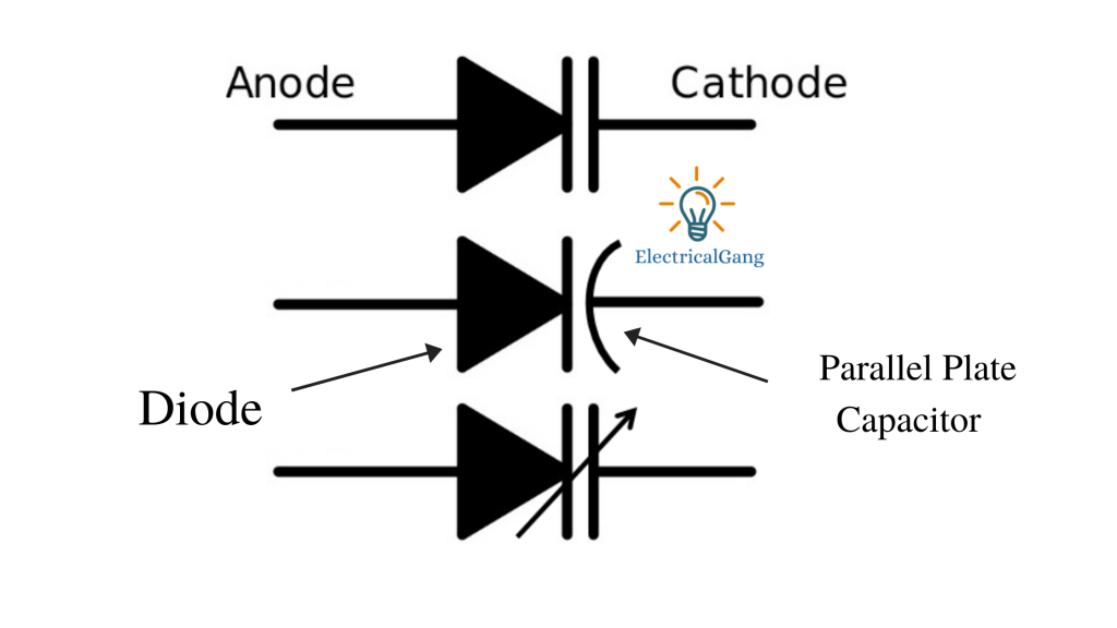
The diode of 2 has the symbol of a capacitor as shown in the figure. The two lines O at the top of the triangle represent the parallel symbol of the capacitor. The 2 parallel lines at both ends of the diode and its other ends show the conductivity of the capacitor The distance between the plates shows their dielectric.
Suggested Read: What Is Light Emitting Diode (LED) | Working Principle of LED
Construction of Varactor Diode:
In Varactor Diode, P-type and N-type are connected using the semiconductor layer. Whose N-type end is attached to the Mesha structure?
The gold-plated molybdenum stud is connected to the N-type layer by a mesa structure and acts as a cathode terminal. The end of the P-type is connected to another gold-plated molybdenum stud (which acts as an anode) by another gold wire. Except for a portion of the molybdenum, the entire system is enclosed in a ceramic layer
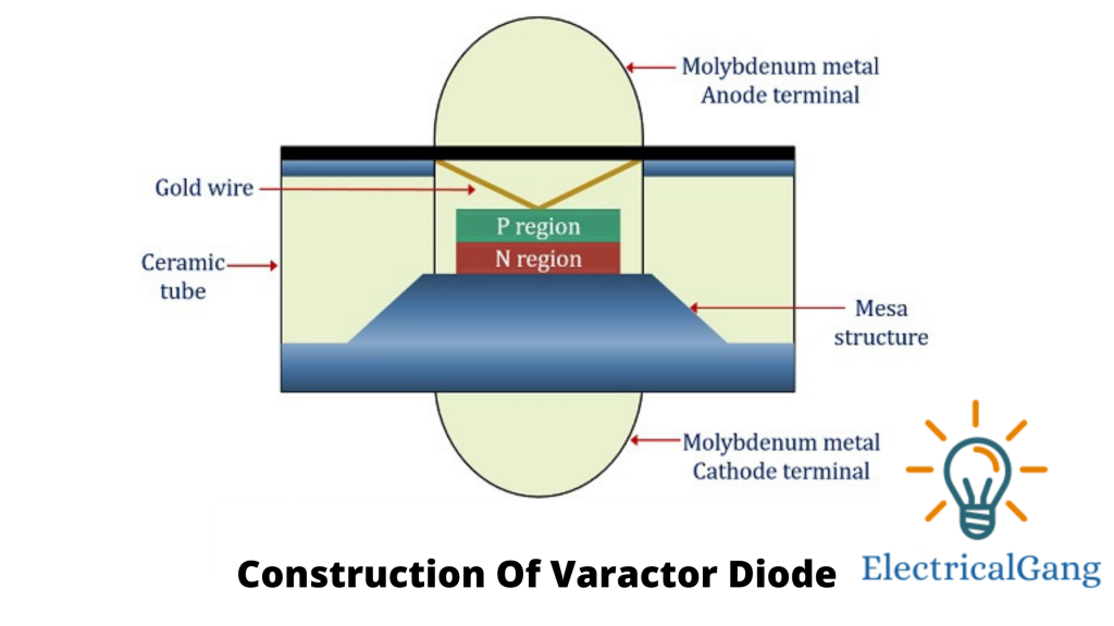
P and N-type layers are mostly made of silicon or gallium arsenide, depending on how it is used. Silicon is used if used for low frequency and gallium arsenide is used if used for high frequency.
The P-type and N-type semiconductor layers are doped with identical impurities to improve conductivity for normal diodes. The concentration of impurities near the junction is very low and gradually increases as we move to the other surface of the layer.
Suggested Read: What is a MOSFET | Construction of MOSFET
Working System of Varactor Diode:
How a Varactor Diode Works First one needs to understand the working principle of a changeable capacitor. The capacitor uses two surfaces that separate from the insulating dielectric. One side is seen from the positive while the other side is connected from the negative. Due to the attraction between the two, a positive charge accumulates on one side and a negative charge on the other side.
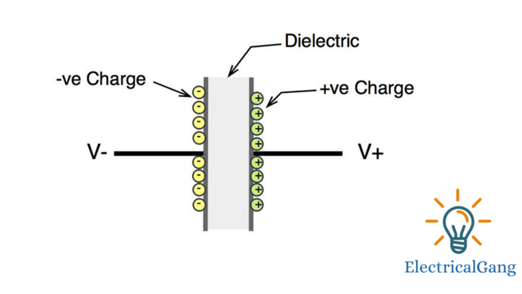
The space, where this charge is collected, is known as capacitance. If the difference between these two surfaces is reduced then the pressure of attraction between these two charge carriers increases and hence more charge accumulates on the surface i.e. capacitance increases.
If the distance between the two is increased. Then there is a reverse process and the capacitance decreases. There is a mechanical facility for this so that we can increase or decrease this distance. Which effectively converts to capacitance.
Let us now go back to the P-N junction. The P-type part is full of positive charge carriers and the N-type part is full of negative charge carriers. The positive and negative charges near the surface of the relationship between the two spread and neutralize each other. This region is known as the depletion zone.
No further propagation of charge carriers through the depletion layer unless a voltage is applied from the outside. So this impressive
The depletion layer acts as an insulator.
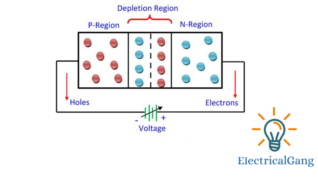
The width of the depletion layer depends on the voltage applied to it. If the forward bias voltage is applied i.e. positive side is applied and the negative side negative voltage is applied then the width of depletion decreases. Above a certain voltage, it disappears completely.
If the opposite voltage is applied in such a way, the width of the depletion layer increases. As shown in the figure below.

Simply put, the depletion region is required by arranging voltage in P&N-type semiconductor layers. The value can be changed. So far we have observed similarities between the capacitor and the diode in the ode bias.
The depletion region level in a diode is like a dielectric medium in a capacitor. Works just like an insulator prevents the flow of charge carriers from one side to the other. When a reverse bias voltage is applied to a diode, these charge carriers converge on both sides of the depletion layer.
Such a diode has some capacitance and is known as junction capacitance. The Varactor Diode is specifically designed to increase this capacity to store charge carriers by allowing it to act as a capacitor.
Suggested Read: What are Semiconductor Devices? | Semiconductor Device Materials
Characteristics of Varactor Diode:
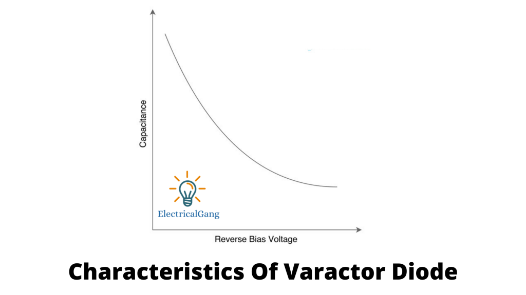
The typical curvature of the Varactor Diode is shown in the figure below. The depletion region increases as the reverse bias voltage increases as shown in the figure. And a decrease in the capacitance of the diode.
Application of Varactor Diode:
Due to the specificity of different voltages and different capacitances, most of the vector diodes are used in frequency modulation or tuning circuits where the value of capacitance determines the manufacture, and modulation frequency.
Some of its uses are as follows:
- Automatic frequency controllers (AFC).
- Frequency multipliers.
- Bandpass filters.
- Harmonic generators.
- Ultra high-frequency television set.
- High-frequency radio.
Like this post? Could you share it with your friends?
Suggested Read –